MIDI Box with Standalone ATMega 328
Background
I wanted to tackle making an embedded microcontroller project in plain C using the ATMega 328 without the Arduino environment [1]. Through school, I had some experience programming the 68HCS12 using Assembly, but I wanted to learn more about developing a project in C for the popular Atmel chips. As an aspiring maker of music widgets - I decided to make a MIDI controller with the following feature set:
- MIDI I/O (in/out/thru) with the 5-pin connector format
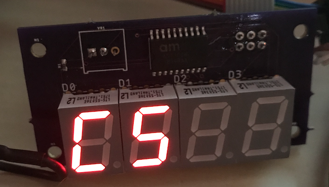
- Four 7-segment LED displays
- LM386 audio amp for modest audio output to power small speakers
- Pinouts to the microcontroller pins for ad-hoc projects i.e. buttons, switches, knobs, etc…
- Microusb to power the project
- 6-pin ICSP (In-circuit serial programmer[2]) header for reprogramming the device. In my case, I’m using an Arudino to program the MIDIBox with an AVR-as-ISP configuration.
Communication
First, I’ll do a brief overview and description of the communication technologies involved in this project assuming a general audience.
UART
Universal asynchronous receiver-transmitter (UART) is a computer hardware device for asynchronous serial communication in which the data format and transmission speeds are configurable[3]. Asynchronous serial communication refers to the data transmission happening through a sequence of bits on an agreed upon rate so no clock line is required. The basic premise behind this communication is a start bit (0 or LOW) which signals the start of data transmission followed by the data of interest (8-bit in our case) which is concluded with the stop bit (1 or HIGH). In this configuration the data needs to be sent at an agreed rate, the baud rate (bit/s), to be properly interpreted. Lastly, the endianness of the receiver/transmitter need to be agreed upon - this refers to the order of bits being sent. For example, Big-endian refers to the most significant bit coming first i.e. 109 where 1 is the Most Significant Bit and 9 the LSB then it would be sent serially as 1 -> 0 -> 9.

For this particular use case, we’ll focus on MIDI.
MIDI
Musical Instrument Digital Interface (MIDI) is a standard that defines the communication protocol widely used in electrical audio instruments [4]. For this discussion, we will assume the MIDI 1.0 protocol. In this configuration, MIDI is an async serial communication protocol where the data frame is a 8-bit word transmitted at 31.25 kbit/s (this was chosen to be the exact division by 1 MHz for compatibility with microprocessors). Wikipedia summarizes the bytes (in hex) we’re interested in here (abridged):
MIDI 1.0 Channel Voice messages
| Event | Status Byte | Byte 2 | Byte 3 |
|---|---|---|---|
| Note Off | 0x8 Channel 0x0..0xF | Note Number | Velocity |
| Note On | 0x9 Channel 0x0..0xF | Note Number | Velocity |
Here the note number can run from 0 to 127 (in decimal) (C1 to G9) and similarly the velocity represents the velocity of striking the keys on a keyboard. The channel message in practice corresponds to having multiple midi instruments on the same port. It’s worth noting that not all midi messages will necessarily be three byte messages (program change event is an example of this).
SPI
Serial Peripheral Interface (SPI) is a synchronous serial communication specification5. It’s a four-wire serial bus with the following wires: SCLK (clock), MOSI (Master Out Slave In - data sent from master), MISO (Master In Slave Out - data sent from slave), SS (Slave Select).
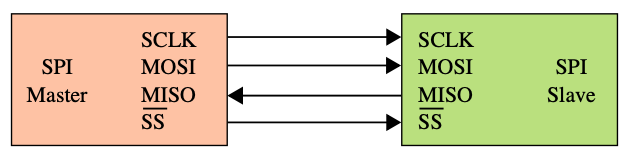
The advantages of this communication configuration:
- there’s no baud rate requirement
- 2-way communication MOSI, MISO
- Multiple devices can communicate on the 2-wire (SCLK, MOSI) same bus leveraging the SS (select) pin.
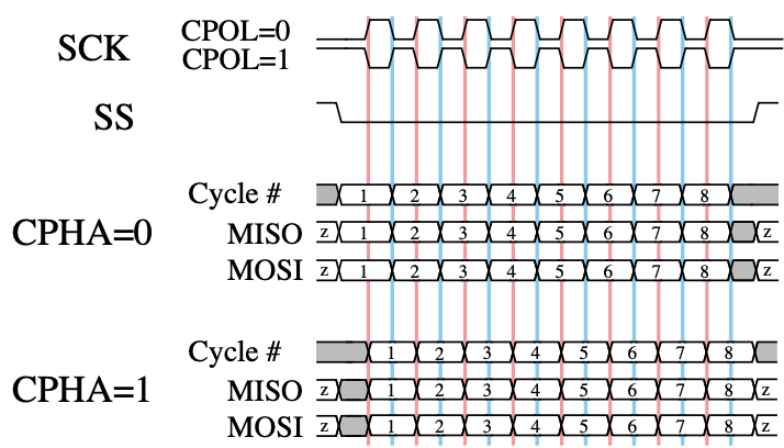
With SPI, there are a few points that need to be configured by the microcontroller regarding the timing and phase of the pin signals. The CPOL (clock polarity - whether the pin idles at LOW or HIGH value) and CPHA (clock phase - whether to read data in on the leading-edge or tailing edge of the trigger) need to be setup. This wiki image visualizes it well:
In my use case, I’m interested in SPI because it’s the communication format used to talk to the AS 1108 chip which is a 4-digit LED (7-segment display) driver6.
Fortunately, the ATMega328p microcontroller has embedded components to handle USART and SPI communication for us without the use of external integrated circut chips. We’ll explore this in the next section.
Software
Configuration on AVR
We’ll look at how to configure the communication on the microcontroller in C. The toolchain used is avrdude to upload the code to the board. In my case, I used an Arduino to flash my MIDI Box board through the ICSP header7. In this section, we’ll lean heavily on the Atmega328p datasheet 8. Additionally, the avr/io.h header file for defining values for the registers of interest. As we’ll see, the registers are the sequence of memory cells (bits) that configure the interrupt systems and read/write data.
Aside on Interrupts
I configured the software to use interrupts 9 which is a system in which a pin change can trigger an immediate execution of code. This allows for more event-driven programming rather than constantly polling for data and state changes. For a great description with examples of configuring interrupts in AVR see: [10]. The interrupt system relies on the hardware (AVR chip) maintaining a list of pointers in memory (vector table). When an interrupt occurs, the function pointed to gets executed. Two notable points of the interrupt system is that the code is blocking the main event loop so you want that to run quickly and there is an ISR (interrupt service routine) table which describes the order of interrupts being serviced/executed (i.e. the order of operations). In my use case, I set up interrupts for UART, SPI, and some basic input controls (switch and potentiometer).
In code there is a global interrupt bit that can be set with sei() to turn on the interrupt system and cli() to clear interrupts globally. These two commands are also handy for running code atomically whenever you need to run a snippet without worrying about interrupts being executed intermittently. Whenever an ISR function is called avr will handle calling cli() at the beginning, to prevent further interrupts from being called within another interrupt, and sei() at the end to allow interrupts to occur again.
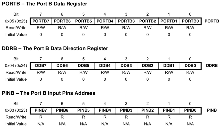
Aside on I/O Ports
A port on the AVR corresponds to an 8-bit storage location that can be accessed as either an input or output. In particular, the 3 register groups of interest are the DDRx, PINx, PORTx where ‘X’ corresponds to the port value B, C, D etc… (refer to chip pinout). The DDR (data direction register) is used for configuring a pin to be either an output or input. The PIN (pin input) corresponds to the input value at each pin number (0-7) for the port of interest. The PORTx register corresponds to the output value to be written to a pin when configured in output mode. Below is an example of PORT D from the data sheet for visual aid.
Communication Setup
I’ll briefly describe the registers and bits of interest in configuring the communication for this project. Reference the datasheet for a more thorough description of the registers.
UART
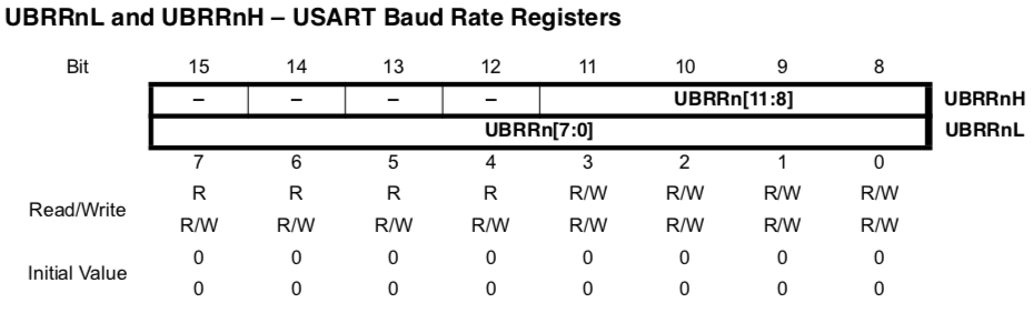
First, I configured the UART baud rate to match the 31.25 kbit/s rate specified by the MIDI protocol. This is done by setting the UBRRnH (the four most significant bits) and UBRRnL (the four least significant bits). The data sheet includes a handy table for realizing what values need to be set here since it’s related to the clock speed on the microcontroller. In my case, I have an external quartz crystal clock at 16 MHz. The avr library includes <util/setbaud.h> which can calculate these values into UBRRH_VALUE and UBRRL_VALUE assuming one’s code defines a BAUD constant and F_CPU (microcontroller clock speed).
In code these are set with:
#define F_CPU = 16000000UL
#define BAUD  = 31250UL

UBRR0H = UBRRH_VALUE;
UBRR0L = UBRRL_VALUE;
Next, we need to configure the USART Control and Status Register n C

The relevant bits here are: UCSZn1 and UCSZn0 which configure the number of bits being framed. In my case, I set both of these values to one with:
UCSR0C = (1 << UCSZ01) | (1 << UCSZ00);
Which sets it to be configured to have 8 data bits and 1 stop bit required for receiving and sending MIDI. Note: UCSZ00 here is a constant storing that bit position within the register so we can bit shift it convienently to turn it on or off.
Now let’s setup the USART Control and Status Register n B.
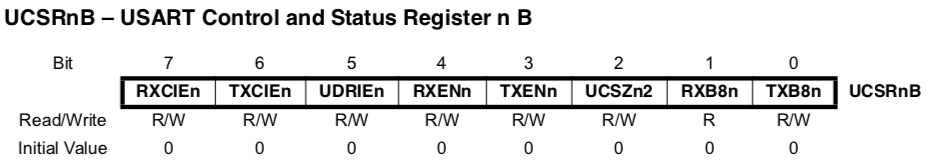
This register handles enabling the receiver/transmitter and interrupt system. In particular we have the following:
- TXENn Transmitter Enable
- RXENn Receiver Enable
- TXENn TX Complete Interrupt Enable
- RXICEn RX Complete Interrupt Enable
As a result:
  UCSR0B = (1 << TXEN0) | (1 << RXEN0); // Turn on RX/TX
  UCSR0B |= (1 << RXCIE0) | (1 << TXCIE0); // Turn on interrupts
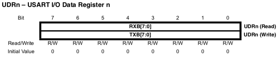
Finally the USART I/O Data Register. These are the two 8-bit registers corresponding to the receive and transmit buffers.
This interrupt configuration allows me to write code like this:
ISR(USART_RX_vect) {
  currentStatePtr->midiRXFlag = 1;
  insertByte(UDR0); // read data
}

ISR(USART_TX_vect) {
  currentStatePtr->midiTXFlag = 1;
  // write
}
~ pg 160 on the microchip datasheet8
SPI
Next I setup the SPI for communicating to the LED display. I set up some basic initialization code:
void initSPI(void) {
  SPI_SS_DDR |= (1 << SPI_SS);                        /* set SS output */
  SPI_SS_PORT |= (1 << SPI_SS);       /* start off not selected (high) */
  SPI_MOSI_DDR |= (1 << SPI_MOSI);                   /* output on MOSI */
  SPI_MISO_PORT |= (1 << SPI_MISO);                  /* pullup on MISO */
  SPI_SCK_DDR |= (1 << SPI_SCK);                      /* output on SCK */
  // Don't have to set phase, polarity b/c default works the CPHA and CPOL table
  SPCR |= (1 << SPR1);                /* div 64, safer for breadboards */
  SPCR |= (1 << MSTR);                                  /* clockmaster */
  SPCR |= (1 << SPE);                                        /* enable */
}
There’s some initialization code for configuring the data direction register and ports as mentioned in the I/O peripheral section.
Focusing on the SPI Control register:
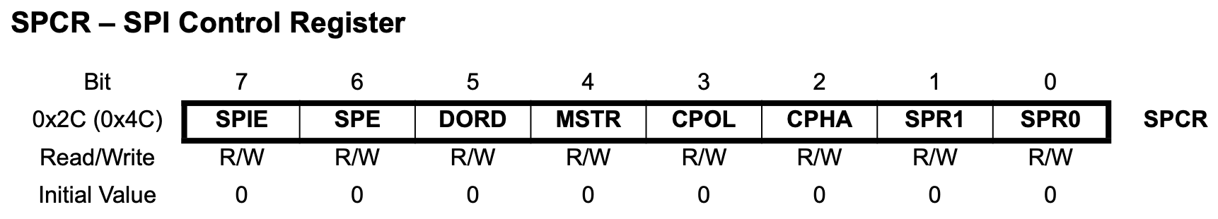
- SPR1 (and SPR0) sets the SCK rate to be div 64 (for F_CPU) in accordance with the data sheet table.
- MSTR (Master/Slave select) sets master SPI mode when written 1 otherwise it’s in slave SPI mode (0).
- SPE (SPI enable) bit enables SPI mode.
- DORD (Data order) a value of 0 means MSB is sent first a value of 1 means LSB is set first. In my case 0 is good.
- SPIE (SPI interrupt enable) a value of 1 sets the interrupt system for serial transfer complete.
void initSPIInterrupt() {
  SPCR |= (1 << SPIE);
}
Finally, the SPI Data Register (SPDR) is the 8-bit register for read/write data transfers.
This allows for the corresponding ISR:
ISR(SPI_STC_vect) {
  SLAVE_SELECT; // signal start transfer
  SPDR = byte; // trade byte
  SLAVE_DESELECT; // signal end transfer
}
~ pg 140 on the microchip datasheet8
Input Peripherals
I set up some basic input peripherals - a switch and knob to control parameters in code. In this section, I’ll discuss how to configure the reading of data from the knob/potentiometer and the state of the switch as well as being notified when changes occur via the interrupt system.
Knob
The knob leverages the ADC system on the microcontroller to map a position of the knob to a value in code. I won’t discuss the ADC system in detail. The gist is that it’s an Analog to Digital Converter (ADC) that can read the analog voltage input from the voltage-divider formed by the potentiometer. The AVR chip holds the 10-bit ADC data which can be read based on the ADC conversion complete interrupt trigger.
void initADC() {
  ADMUX |= (1 << REFS0); // reference voltage on avcc
  ADMUX |= (1 << ADLAR); // left adjust result
  ADCSRA |= (1 << ADPS2) | (1 << ADPS1); // adc clock prescalr / 64
  ADCSRA |= (1 << ADEN); // enable adc
}

void startADC() {
  ADCSRA |= (1 << ADSC); // start the adc conversion
}
Let’s dive into the corresponding registers in the datasheet to understand what’s happening.
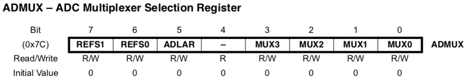
The ADC Multiplexer Selection Register (ADMUX) is for multiplexing the ADC inputs so that multiple ADC inputs can update the value of the ADC data register. In my case, I only have one ADC pin being read so I just set the REFS0 bit which sets up the reference voltage on AVCC with external capacitor at AREF pin. This allows for analog values to be read against some reference voltage that defines the max value.
The ADMUX register also contains the ADLAR bit (ADC Left Adjust Result). This bit impacts how the high and low bits of ADC data are represented in the ADCL and ADCH registers. Since the ATMega328p has a 10-bit register the resulting value is found in these two registers.
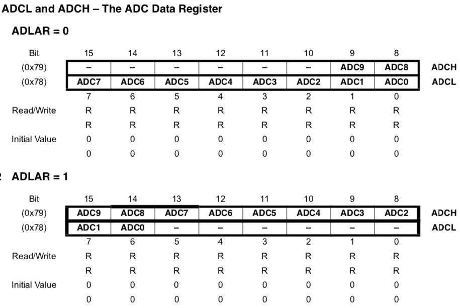
For now I only care about the 8 most significant bits so I’ll set the ADLAR bit so I can read the ADC data by just grabbing the value of ADCH.
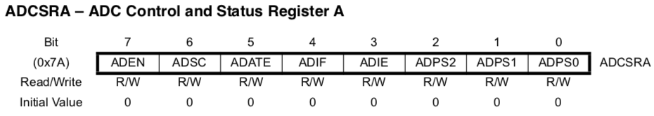
The ADC Control and Status Register A (ADCSRA) is critical for setting up the interrupt system and reading data.
- ADEN bit being set to 1 will enable the ADC
- ADIE bit being set to 1 will enable the ADC interrupt
- ADSC bit starts the ADC conversion. The ADC can run in single conversion mode (read once per bit set) or free running mode (constantly running after the first start).
- ADPS2, ADPS1, ADPS0 bits are for selecting a prescalar for the ADC clock. This means it’ll divide the cpu clock speed by a factor and have that be the ADC clock speed. I don’t need particularly quick results so I set ADPS2 and ADPS1 to get a factor of 1/64.
To respond to knob changes immediately I setup the ADC interrupts
void initADCInterrupt() {
  // Enable ADC interrupts
  ADCSRA |= (1 << ADIE);
}

ISR(ADC_vect) {
  currentStatePtr->knobFlag = 1;
  currentStatePtr->knobValue = ADCH; // drops 2 bits of precision as discussed
  startADC(); // trigger the next read
}
~ pg 217 on the microchip datasheet.
Switch
The switch functions by setting up a pin change interrupt on the chip which then has a bit that can be read to differentiate the LOW and HIGH state of the switch (grounded vs +5V).
void initInterrupt0(void) {
  EIMSK |= (1 << INT0);
  EICRA |= (1 << ISC00);
}
Taking a closer look at the corresponding registers, we have:
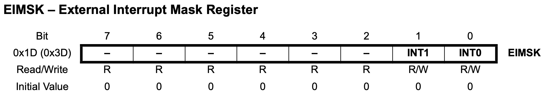
The INT0 bit sets the external interrupt triggered on the rising/falling edge of pin INT0.
and
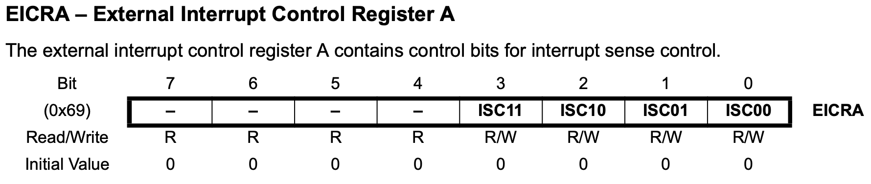
The ISC00 bit on External Interrupt Control Register A (EICRA) will configure the interrupt to trigger on both a rising and falling edge. Other combinations of bits to ISC00 and ISC01 can be set to trigger on just a rising edge or falling edge instead.
Setting up these interrupts allows me to write code like this:
ISR(INT0_vect) {
  if (bit_is_clear(SWITCH_PIN, SWITCH)) {
	currentStatePtr->switchValue = 1;
  } else {
	currentStatePtr->switchValue = 0;
  }
  currentStatePtr->switchFlag = 1;
}
~ pg 54 in the microchip datasheet.
Source: https://github.com/jescriba/MIDIBox/tree/master/Software
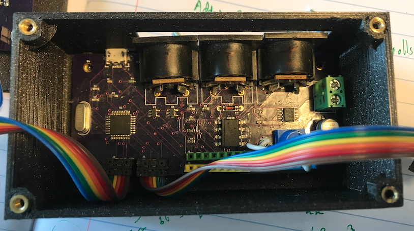
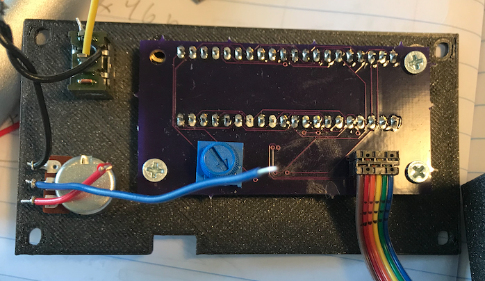
MIDI Box Circuit
Next, I’ll describe the actual schematic and PCB design for the MIDI box circuit.
Fig. 1
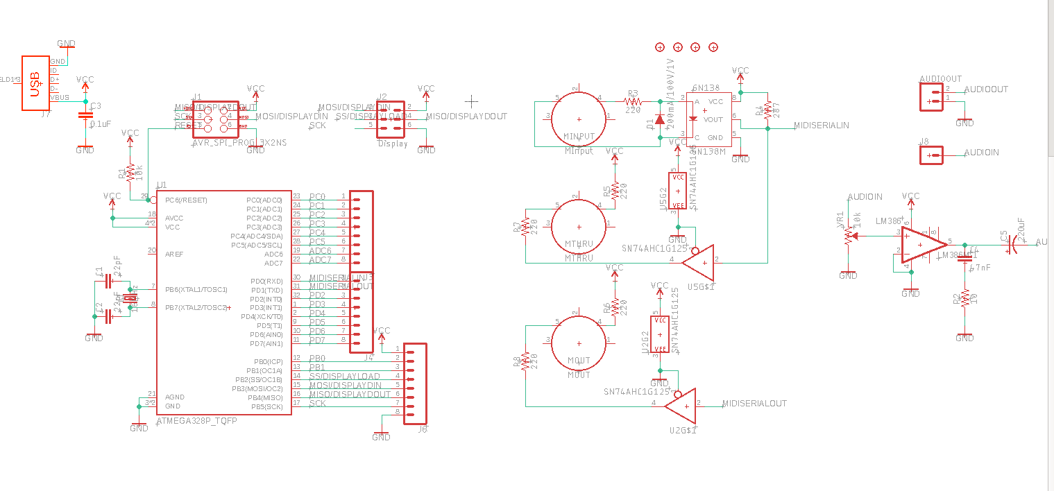
Fig 2.
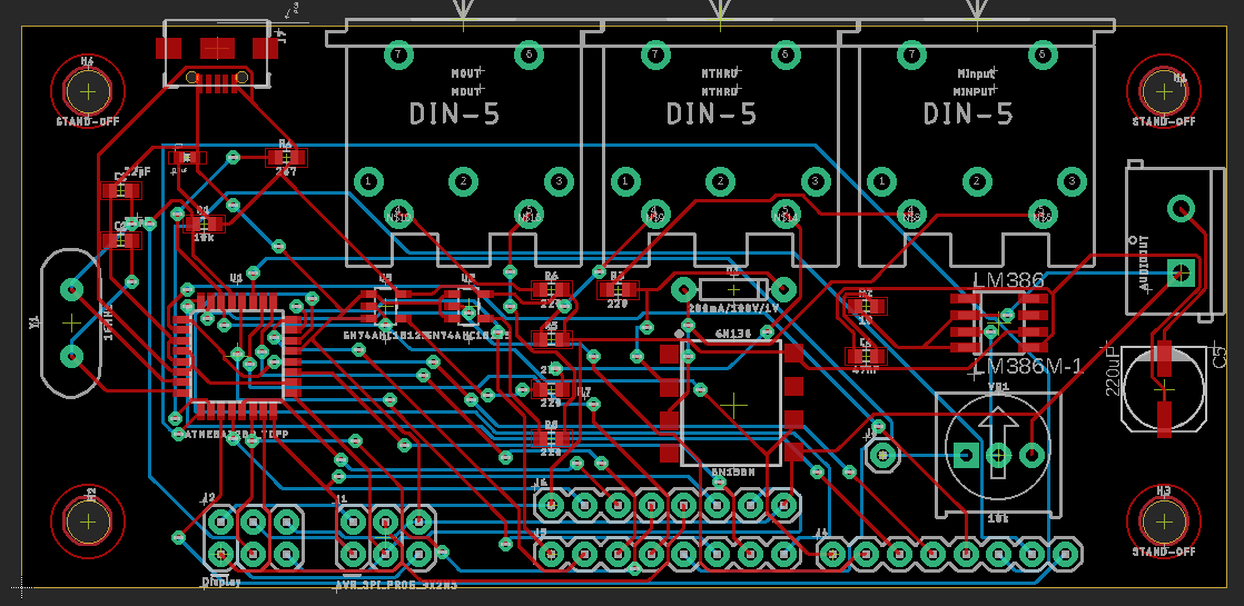
It’s a fairly derivative circuit, but I’ll review the basic pieces.
At the top left fig 1 is the microusb surface mount component used to power the project. Included in the powering component is a capacitor to filter fluctuations in the power supply (more isolation is certainly needed…).
The center left fig 1 is the ATMega328p surface mount chip with an external quartz crystal clock. The microcontroller’s pins are connected to a breakout pinout. Additionally, chip is setup to allow for programming via the ICSP 6-pin header and another 6-pin header for SPI communication to the LED display board (AS 1108 + 4-digits).
In the center fig 1 is the unit for MIDI I/O. It’s the suggested circuitry in the MIDI docs for setting up IO. The notable components are buffers to isolate the circuit, 6N138 optocoupler (for isolating MIDI input since the coupler removes the physical connection using optics), and a reverse diode for protection against input reversely biased.
On the far right fig 1 is a standard LM386N IC chip which is a low power audio amp. It’s output is ac coupled for audio output.
Lastly, there’s standoffs on the PCB to mount it to the enclosure.
Source: https://github.com/jescriba/MIDIBox/tree/master/Hardware
Debugging
Considering this project is certainly a prototype, I had to debug the circuit to understand issues as we’ll see…
Oscilloscope debugging
I setup my Rigol oscilloscope to read both UART (MIDI) and SPI (Display). This setup was useful for validating the messages from the microcontroller and inspecting signal integrity. Additionally, it’s handy to visualize the timing diagram with real hardware.
This image displays all of the communication happening (UART + SPI). The blue line highlighted parameter is the MIDI receive line configured to display in hex. The yellow line is the SPI clock.

Below is a closer photo of strictly the SPI communication. Here the SCLK is yellow, SS is pink, MOSI is blue. The data in this example is being displayed in binary.

Transient Loading
One issue I noticed with the circuit is noise on the power lines. This noise causes an unbearable hiss/buzz when the speaker is plugged into the circuit.
![]()
Judging from the photo the issue seems to be from the clock on the LED driver for multiplexing (cycling through the segments to display in the kHz domain). This can be verified by turning off the LED display and observing the audible noise vanishing. The multiplexing results in a quickly changing load on the power supply for the circuit resulting in the transient loading issues where the corresponding voltage fluctuates periodically as a result of the increased or decreased demand for current from the display (resistive load)11.
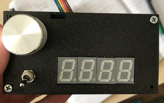
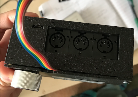
Enclosure Design
Finally, I designed an enclosure for the printed circuit board using Blender 12. I used heat threaded insets for screwing in the display to the lid and the circuit to the base. I was able to print the design with a 3D printer and with a little bit of modification got this result:
Blender Source included in hardware: https://github.com/jescriba/MIDIBox/tree/master/Hardware
Conclusion
Software Improvements
One noteworthy software improvement would be using the timer system on the AVR chip to have 8-bit synth audio output. Another improvement would be to add additional I/O peripherals like knobs, switches, buttons, motors, etc, etc… I’ll likely follow up on additional software improvements since that’s something that can be delved into significantly.
Hardware Improvements
Upcoming hardware improvements include: fixing the transient loading issue by isolating the display with capacitors or a buffer, adding a usb to serial chip for directly programming via usb, and improving the trace layout and routing on the PCB (I used the auto-router..).
References
https://www.oreilly.com/library/view/make-avr-programming/9781449356484/ [1]
https://en.wikipedia.org/wiki/In-system_programming [2]
https://en.wikipedia.org/wiki/Universal_asynchronous_receiver-transmitter [3]
https://en.wikipedia.org/wiki/MIDI [4]
https://en.wikipedia.org/wiki/Serial_Peripheral_Interface [5]
https://ams.com/documents/20143/36005/AS1108_DS000169_2-00.pdf/dbb78f28-8ed1-b338-3144-d8af7e76a4b8 [6]
https://github.com/jescriba/MIDIBox/tree/master/Software [7]
https://www.sparkfun.com/datasheets/Components/SMD/ATMega328.pdf [8]
https://en.wikipedia.org/wiki/Interrupt [9]
http://bytes.usc.edu/files/ee109/slides/EE109Unit12_Interrupts.pdf [10]
https://micro.rohm.com/en/techweb/knowledge/dcdc/dcdc_sr/dcdc_sr01/1632/ [11]
Background Jobs with Resque
Background
I wanted to do a quick review of setting up background jobs for a Sinatra app I have deployed with Heroku. My web app serves as a music archive where I can upload songs for reference. Naturally, I wanted the site to be able to handle lossless audio formats so I could have acccess to both the lossless and lossy formats. This is where Resque comes in. Resque is a Redis-backed Ruby library for creating job queues, and Redis is an open source (BSD licensed), in-memory data structure store, used as a database, cache and message broker. In my example, I set up a jobs queue for transcoding my lossless audio formats to mp3 using ffmpeg. In this post, I’ll show you how I got Sinatra, ffmpeg, Resque, and Redis working together in Heroku.
RESTful Music Archive
A RESTful music archive with Sinatra that handles lossless and lossy audio formats.
Source: https://github.com/jescriba/music-archive
Setting up Resque
After installing and requiring the resque gem, I added some uploading logic to my route POST to artists/:id/songs that checks if the uploaded file format is of type audio/x-aiff among other lossless formats.
References: POST to artists/:id/songs Upload Song
To queue up the transcoding logic, I call: Resque.enqueue(SongTranscoder, upload_params) after the initial upload. The rest of the logic lives inside my SongTranscoder and Rakefile. Resque will automatically call the class perform method. In this method, I download the lossless file from s3 then shell out to ffmpeg to transcode to mp3.
  def self.perform(upload_params)
    s3 = Aws::S3::Resource.new(region: 'us-west-1')

    # Ensure we are working w/ symbols
    upload_params = upload_params.reduce({}) { |memo, (k, v)| memo.merge({ k.to_sym => v}) }
    extension = File.extname(upload_params[:lossless_url])
    # Download s3 lossless to local
    upload_params[:tempfile_path] = "/app/tmp/temp#{extension}"
    download_cmd_str = "curl -o #{upload_params[:tempfile_path]} #{upload_params[:lossless_url]}"
    download_cmd =  `#{download_cmd_str}`
    tempfile = File.new(upload_params[:tempfile_path], "r")

    # transcode to V0 mp3
    temp_fi_dirname = File.dirname(upload_params[:tempfile_path])
    lossy_file_path = "#{temp_fi_dirname}/#{upload_params[:song_name]}.mp3"
    cmd = "ffmpeg -i #{upload_params[:tempfile_path]} -codec:a libmp3lame -qscale:a 0 #{lossy_file_path}"
    `#{cmd}`
    lossy_file = File.new(lossy_file_path, "r")

    # upload lossy
    lossy_object_path = upload_params[:lossy_url].sub(upload_params[:base_url], "")
    s3_lossy_object = s3.bucket(BUCKET).object(lossy_object_path)

    # upload
    s3_lossy_object.upload_file(lossy_file, acl: 'public-read')
    s3_lossy_object.copy_to("#{s3_lossy_object.bucket.name}/#{s3_lossy_object.key}",
                            :metadata_directive => "REPLACE",
                            :acl => "public-read",
                            :content_type => "audio/mpeg",
                            :content_disposition => "attachment; filename='#{upload_params[:song_name]}.mp3'")

    # Clean up lossy temp file
    FileUtils.rm(lossy_file_path)

    # Clean up - delete temp file
    FileUtils.rm([upload_params[:tempfile_path]])
  end
References: SongTranscoder
Setting up Resque Server
Resque comes with an easy to set up server that’ll be helpful for monitoring jobs.
In my config.ru file, I map the /resque route to the Resque server:
require 'resque/server'
require_relative 'main'
require_relative 'globals'

$stdout.sync = true

map "/resque" do
  Resque::Server.use Rack::Auth::Basic do |username, password|
    [username, password] == [Globals::AUTH_USER, Globals::AUTH_PASSWORD]
  end

  run Resque::Server
end

map "/" do
  run Main
end
Configuring Heroku
Add Worker Dyno
Next I added a worker dyno for running the queue of jobs from the Rakefile:
QUEUE=* RACK_ENV=production bundle exec rake resque:work
Add Redis To Go
In my Rakefile and Globals, I set up Resque per rack environment to use different redis servers:
if ENV["RACK_ENV"] != 'production'
  Resque.redis = 'localhost:6379'
else
  uri = URI.parse(ENV["REDISTOGO_URL"])
  Resque.redis = Redis.new(:host => uri.host, :port => uri.port, :password => uri.password)
end
Note: I set REDISTOGO_URL in my Heroku environment variables to that specified by the Heroku Redis To Go Add-On.
Add Ffmpeg Build Pack
Lastly, to get ffmpeg to actually work on Heroku, I added an ffmpeg build-pack.